

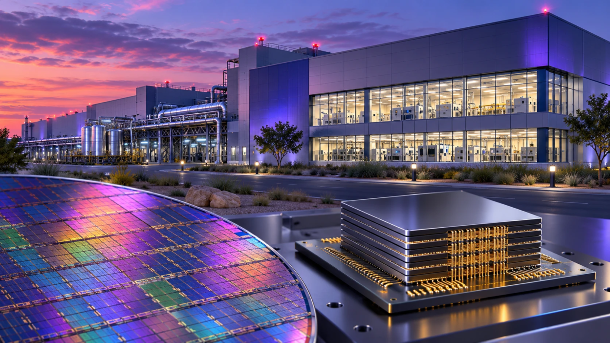
Samsung Electronics is reportedly preparing to expand its semiconductor manufacturing operations in Texas, United States, with plans to produce advanced memory chip components for technology giants AMD and Nvidia. The South Korean company is expected to use its second chipmaking facility in Taylor, Texas, to manufacture important parts of high-bandwidth memory (HBM) chips, which are widely used in artificial intelligence systems and powerful data centers.
On November 3, 2026, South Korea’s Maeil Business Newspaper reported, citing industry sources, that Samsung had secured orders for the planned Taylor Fab 2 facility. According to the report, AMD is expected to account for most of the proposed high-bandwidth memory base-die production, while Nvidia was also named among the intended customers. Samsung said it could not confirm customer-related details, and the specific manufacturing arrangements have not been publicly confirmed by the companies.
The proposed manufacturing facility, known as Taylor Fab 2, would reportedly use Samsung’s advanced 2-nanometer (2nm) semiconductor process for future chip components. The 2nm designation refers to a generation of chip manufacturing technology rather than the exact physical size of every transistor. Advanced manufacturing processes can help improve chip performance, power efficiency and transistor density. According to the report, the second factory would cover approximately 2.7 million square feet, making it about 1.5 times larger than Samsung’s first Taylor facility.
According to the reported schedule, construction of the second factory is expected to formally begin in November 2026. Manufacturing equipment could start arriving in February 2029, while large-scale chip production is planned for 2030. These dates show that the project is focused on meeting future semiconductor demand rather than immediately increasing the supply of AI chips.
One of the main products expected from Taylor Fab 2 is the base die used in high-bandwidth memory (HBM). This specialized logic chip sits underneath stacked memory chips and helps manage communication between the memory and a powerful processor. According to Samsung’s HBM4 product specifications, its current HBM4 technology uses a 4nm logic base die. The reported 2nm manufacturing plan concerns a future generation of these components. HBM is especially important for AI training, high-performance computing and data centers because it allows processors to access large amounts of data at high speed.
Samsung and AMD already have an established relationship in advanced AI memory technology. In March 2026, the companies announced an expanded strategic collaboration covering HBM4 memory for AMD Instinct MI455X AI accelerators, along with other memory technologies and possible foundry cooperation. Both AMD and Nvidia rely on high-performance memory to help their processors handle demanding AI workloads, including model training, image processing and large-scale data analysis. However, the earlier Samsung-AMD announcement does not confirm a separate manufacturing agreement for Taylor Fab 2.
Nvidia’s possible involvement requires additional caution. The November 3 report also said Nvidia had asked memory suppliers to use Taiwan Semiconductor Manufacturing Company (TSMC) to produce base dies for a customized memory design called NVHBM. Samsung is reportedly examining whether its own foundry could manufacture some of those components if TSMC faces capacity limitations. As a result, the report should not be interpreted as confirmation that Nvidia has selected Samsung’s Texas factory to produce all its future HBM base dies.
Samsung’s reported expansion could also strengthen its position in the competitive semiconductor manufacturing industry. The company operates both memory-chip and foundry businesses, meaning it can manufacture its own chips while also producing semiconductor components for other companies. Securing orders from major AI hardware developers would support its efforts to attract more advanced manufacturing customers.
Samsung has already secured a major manufacturing agreement involving Tesla at its first Taylor facility. In July 2025, the company entered a $16.5 billion semiconductor supply agreement with Tesla covering future AI chips. The proposed Taylor Fab 2 project would expand Samsung’s manufacturing presence in Texas and could help the company serve additional customers developing next-generation computing hardware. It would also strengthen efforts to increase advanced semiconductor production capacity in the United States.
The reported project comes as semiconductor companies face growing pressure to increase production capacity for AI-related hardware. Competition is also increasing among memory manufacturers, including Samsung, SK Hynix and Micron, as demand for advanced HBM technology grows. Micron’s development of HBM4 memory for AI computing reflects this wider industry trend. Meanwhile, major AI infrastructure projects, including HPE’s $1.2 billion AMD Helios infrastructure order, show how companies are preparing to deploy more powerful computing systems. These investments help explain the long-term demand Samsung hopes to serve through its proposed Texas expansion.
Several important details remain unconfirmed. Samsung has not verified the specific customer arrangements reported for Taylor Fab 2, and the companies have not publicly disclosed detailed order volumes, contract values or manufacturing commitments for the proposed facility. Questions also remain about the extent of Nvidia’s involvement and which future HBM designs would use Samsung-made base dies. Although the reported schedule targets mass production in 2030, construction progress, equipment installation and customer requirements could affect the final timeline.
For now, Samsung’s reported Texas expansion highlights the growing importance of advanced memory technology in the global AI industry. If the proposed arrangements move forward, the Taylor facility could become an important production center for components supporting future AMD and Nvidia AI hardware, while strengthening semiconductor manufacturing capacity in the United States.


