


AI accelerators keep gaining computing power, but moving data efficiently between chips, memory, and racks remains a major challenge. Optical interconnects help address this problem by transmitting information as light through optical fibers or waveguides. They are already widely used in data center networking, while optical connections integrated closer to processors are an emerging technology. Their main advantage is the ability to support high-bandwidth communication over suitable distances while potentially reducing power consumption.
What is an Optical Interconnect?
An optical interconnect is a communication link that uses photons to transmit data through optical waveguides such as fiber or on-package waveguides. It replaces or augments copper traces that move bits as electrical signals across a board, backplane, or cable.
Optical interconnects should not be confused with photonic computing. Optical interconnects focus on transmitting information between components, while photonic computing explores using light to perform selected calculations. Understanding this difference helps explain why optical networking is already established in data centers, while broader light-based computing remains an emerging field.
In practice, an optical interconnect is a complete communication system rather than a single component. A laser generates light, a modulator encodes electrical data onto the optical signal, and a fiber or waveguide carries that signal to its destination. A photodetector and receiver circuitry then convert it back into an electrical signal that conventional processors can use. These conversion stages consume power, so the efficiency of the complete link matters more than the optical transmission alone.
Why Do AI Chips Need Optical Interconnects?
Many AI workloads are limited by how quickly data can move between processing units, memory, and other accelerators. During training and inference, GPUs repeatedly access model weights, activations, and other data needed for complex mathematical operations. High-bandwidth memory (HBM) usually communicates with processors through short electrical connections, while optical interconnects are especially useful for high-bandwidth communication across longer distances. Researchers are also developing optical input/output technologies that could bring light-based connections closer to processor packages.
Electrical links run into limits as speeds rise. Signal loss, crosstalk, and equalization overhead increase sharply with distance and data rate, which drives power and heat while constraining reach.
The communication requirements of AI infrastructure also depend on the workload. Large training clusters often prioritize sustained bandwidth for communication between GPUs, while inference systems may place greater emphasis on response time and predictable service performance. Our guide to training and inference AI data centers explains how these different priorities influence networking, memory, and hardware architecture.
- Higher Aggregate Bandwidth: Optics can scale using multiple wavelengths and parallel fibers, supporting very high throughput between nodes.
- Lower Energy per Bit at Suitable Distances: Optical links can reduce the energy needed to move data over longer or higher-bandwidth connections. However, total power consumption must include lasers, drivers, receivers, and any required signal processing.
- Better Signal Integrity: Light is less sensitive to electromagnetic interference, helping optical channels maintain signal quality in dense computing environments.
- Higher-Density Rack Connections: Optical fibers support high-bandwidth communication across racks while helping manage dense network connections. However, the overall efficiency of an AI network still depends on its switch architecture, traffic management, and software.
These advantages matter most when systems must scale out across many accelerators and racks while staying within strict power and cooling budgets.
Key Components Inside an Optical Interconnect
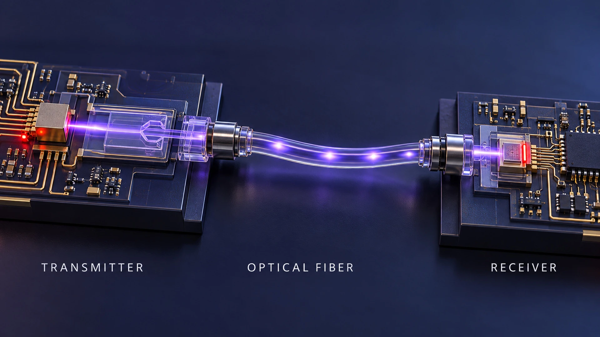
Understanding the building blocks helps clarify why optics can change system design. Each block has its own constraints and tradeoffs that affect performance and cost.
Transmitter and Modulator
The transmitter provides light and the modulator encodes electrical data onto that light. Designs may use integrated lasers or external lasers coupled into the module, depending on thermal goals and packaging complexity.
Modulation formats and line coding influence bandwidth and error tolerance. Higher speeds can demand more careful control of noise, temperature drift, and component variation.
Waveguides and Fiber
Optical signals travel through fiber, through waveguides on a substrate, or through short on-package routes. The choice affects insertion loss, bend radius limits, connector design, and manufacturability.
Connectors and alignment are critical because even small mechanical errors can create significant loss. That is one reason packaging and assembly are central to successful optical deployments.
Receiver and Photodetector
The receiver converts light back into an electrical signal using a photodetector and amplification chain. Sensitivity and noise performance determine how much optical power is required and how far a link can reach.
At high data rates, clock recovery and forward error correction help maintain reliable communication by detecting or correcting transmission errors. However, these functions can introduce additional power consumption, processing complexity, and latency, so engineers must balance reliability with system performance.
Optical Interconnects vs. Electrical Interconnects
Optics is not a universal replacement for copper. The best choice depends on reach, bandwidth density, power constraints, and the cost target of the platform.
| Attribute | Electrical Interconnect | Optical Interconnect |
|---|---|---|
| Typical Strength | Low cost and simple for short reach | Scales bandwidth well across longer reach |
| Distance Behavior | Loss and equalization demands rise with reach | Lower transmission loss over suitable longer reaches |
| Power at High Speed | Re-timers and equalizers can add power | Can offer better energy per bit at suitable distances, including conversion overhead |
| Integration Challenges | Routing density and crosstalk limits | Packaging, alignment, and optical coupling |
| Additional Components | May require equalization or re-timing at high speeds | Requires optical transmitters, receivers, and light sources |
The practical design question is where the crossover point sits for a given architecture. Many modern systems use electrical links within a package or board and optics for longer runs between boards, trays, or racks.
High-speed electrical interconnects remain important in modern AI systems. For example, NVIDIA’s NVLink Fusion technology supports connections between different types of processors and accelerators within specialized AI infrastructure. This illustrates why optical and electrical technologies should be evaluated as complementary options rather than direct replacements in every situation.
Where Optical Interconnects Show Up in AI Systems?
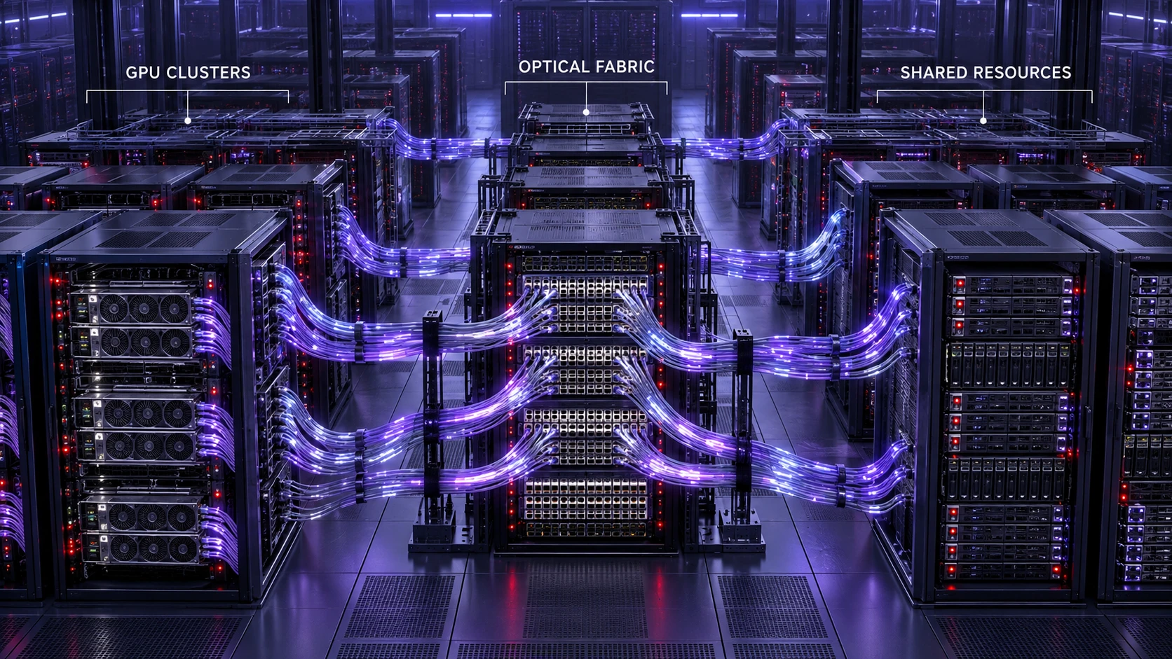
Optical connectivity is commonly used to build high-bandwidth fabrics between accelerator nodes and across data center networking layers. It supports scale-out patterns that distribute training across many nodes.
One real-world example is NVIDIA’s co-packaged optics architecture, which integrates silicon photonics engines with high-performance networking switches. The design uses optical connections to support large AI infrastructure while addressing bandwidth density, power efficiency, and system reliability. It also illustrates the importance of lasers, optical packaging, and manufacturing when building advanced AI networks.
Optical interconnects may also support disaggregated computing architectures, where processing resources, memory, and storage are separated into shared pools rather than being contained within a single server. High-bandwidth optical links can help connect these resources across racks, but practical performance also depends on communication protocols, memory access latency, and system software. Not every resource can be efficiently separated from a processor, especially when applications require extremely fast memory access.
- GPU and Accelerator Clusters: Optical links connect nodes through high-speed network adapters and switches.
- Rack-Scale Fabrics: Optical cabling supports dense spine-and-leaf network designs with many parallel connections.
- Shared AI Infrastructure: High-capacity optical networks can support multiple AI workloads across shared data center resources. However, workload isolation and predictable performance require appropriate network configuration, traffic management, and software controls.
Placement is driven by reach and bandwidth density, not by a single rule. As packaging improves, optics can move closer to the die to reduce electrical trace length and improve efficiency.
The broader shift toward integrated AI hardware can be seen in HPE’s AMD Helios AI infrastructure, which combines GPU accelerators, networking equipment, and cooling systems in a rack-scale platform. Although the system illustrates high-bandwidth AI networking rather than proving that every connection uses optics, it demonstrates why networking and compute hardware must be designed together.
Packaging and Architecture Trends Driving Adoption
Advanced semiconductor packaging allows more processing components to fit within compact systems, increasing the demand for high-bandwidth connections. Chiplets and multi-die processors must exchange large amounts of data with minimal delay, but many of these short-distance connections still use electrical interfaces. Optical input/output technology is being developed as another option for selected high-bandwidth connections where electrical signal loss, routing density, or power consumption becomes a limitation.
Optical I/O is increasingly discussed alongside co-packaged optics, pluggable optics, and near-package optical engines. Each approach balances serviceability, thermal constraints, and total cost of ownership.
A practical example comes from Intel’s optical compute interconnect chiplet, which was demonstrated alongside a CPU in 2024. The prototype supports high-bandwidth optical communication and shows how photonics could eventually move closer to computing hardware. However, the demonstration should not be confused with widespread commercial deployment of optical interfaces inside AI processors.
Pluggable Optics
Pluggable modules are familiar in data centers because they are replaceable and fit existing operational models. They tend to sit at the edge of the board, which can require longer high-speed electrical traces between the chip and the module.
That electrical reach can become a limiting factor at higher lane rates. Designers may need re-timers or additional signal conditioning that adds power and complexity.
Co-Packaged and Near-Package Optics
Near-package optics places optical engines close to a processor or switch package, reducing the distance that high-speed electrical signals must travel. Co-packaged optics (CPO) goes further by integrating optical engines within the same package as the main processing or switching chip. Both approaches aim to improve bandwidth density and reduce electrical signal losses, but they differ in packaging complexity, cooling requirements, and maintenance options.
The tradeoff is integration complexity and serviceability. Thermal management and manufacturing yield become more significant concerns when optics sits near hot silicon.
These tradeoffs are illustrated by Cisco’s co-packaged optics demonstration, which explains how shorter electrical connections can reduce power consumption. Cisco also describes the use of external laser sources to keep heat-sensitive components away from the main switching chip and make laser replacement easier. This highlights why thermal design and maintenance access are important considerations for optical networking hardware.
Latency, Bandwidth, and Power Considerations
AI training often requires high network bandwidth to exchange data and synchronize work across many accelerators. AI inference may place greater emphasis on response times, particularly when applications must generate results quickly. Optical interconnects can support both workloads by enabling high-capacity communication, but they do not automatically reduce latency. Actual performance depends on switching delays, network congestion, electrical-to-optical conversion, signal processing, and the overall network architecture.
Power is a system-level topic. Even if an optical link reduces energy per bit over reach, lasers, drivers, and digital signal processing (DSP) functions still consume power, and their heat must be removed reliably.
- Link Budget Discipline: Managing insertion loss, connector loss, and receiver sensitivity helps avoid unnecessary laser power consumption while maintaining adequate signal margin.
- Topology Efficiency: Well-designed network fabrics distribute traffic efficiently and reduce congestion caused by oversubscribed connections. This can improve effective throughput and reduce communication delays during demanding AI workloads.
- Thermal Planning: Keeping optics within their operating temperature limits preserves wavelength stability and helps control error rates.
When these variables are tuned together, optics can help deliver more usable bandwidth per watt for distributed AI.
Challenges and Tradeoffs to Know
Optical interconnects introduce new engineering concerns that many teams do not face with copper. The most common issues involve packaging, testing, and operational practices.
- Manufacturing and Alignment: Coupling light efficiently requires precise alignment and robust connectors.
- Reliability and Monitoring: Systems need telemetry for optical power, temperature, and error rates to detect degradation early.
- Cost and Supply Chain: Lasers, photonics packaging, and high-volume testing can affect platform economics.
- Standardization Pace: Optical interfaces, laser modules, and packaging designs continue to evolve. Industry specifications such as OIF’s co-packaging implementation agreements help define interoperable components and interfaces. Organizations planning long-term deployments should evaluate standards support, vendor compatibility, and future upgrade requirements.
These constraints are manageable, but they require cross-functional design across silicon, packaging, networking, and data center operations.
How to Evaluate Optical Interconnect Options?
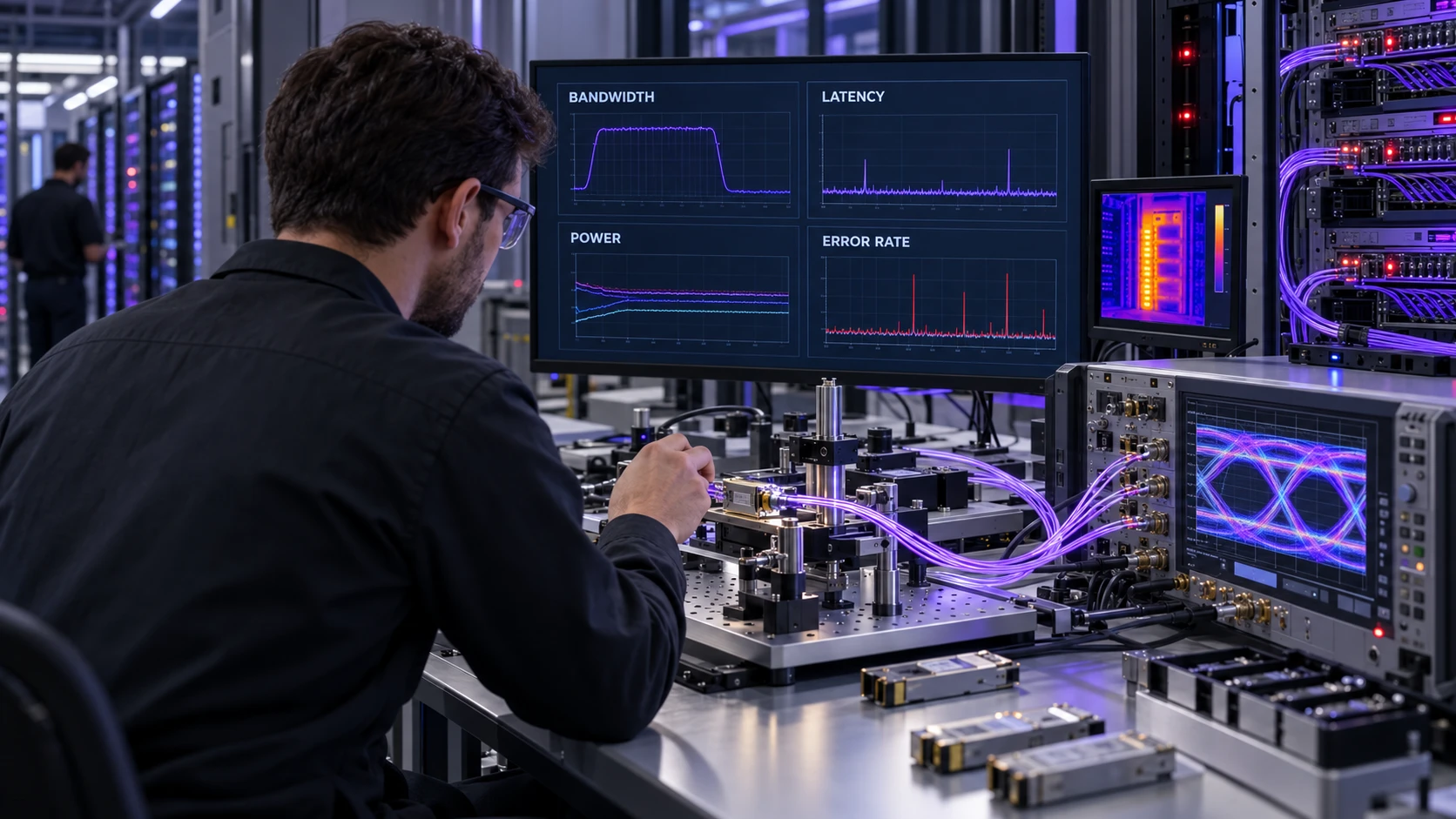
A good evaluation starts with workload requirements and ends with an end-to-end fabric plan. Focusing only on peak link speed can lead to disappointing results if topology, oversubscription, or software collectives are weak.
- Define Communication Needs: Quantify bandwidth, latency, and message patterns for training and inference.
- Map the Reach Profile: Separate on-package, on-board, rack, and inter-rack distances to find where optics delivers the biggest return.
- Model Power and Cooling: Include optics, DSP, re-timers, and switch power in total cost of ownership estimates.
- Check Operability: Ensure monitoring, replacement workflows, and diagnostics fit the operating model.
- Validate With Stress Testing: Test worst-case temperature, vibration, and error conditions to confirm margin.
This sequence keeps the decision grounded in measurable system outcomes rather than marketing numbers.
Conclusion
Optical interconnects use light to transmit data across high-bandwidth communication links, helping AI infrastructure overcome some of the distance, signal loss, and power limitations associated with electrical connections. They are especially valuable in large data center networks that support distributed AI training and inference. However, the best choice between optical and electrical technology depends on connection distance, bandwidth requirements, system cost, and overall energy efficiency.
The biggest gains come from treating optics as part of a complete architecture that includes packaging, fabric topology, monitoring, and cooling. With careful design, optical interconnects help AI platforms scale performance while staying within power and reliability constraints.
Frequently Asked Questions
Is An Optical Interconnect Always Faster Than Copper?
Not always. Over very short distances, copper can be efficient and simpler, and overall performance depends on the complete link design. Optics tends to pull ahead as reach and bandwidth density increase and electrical signal conditioning becomes costly.
Do Optical Interconnects Reduce Latency for AI Workloads?
Not automatically. Optical interconnects can support low-latency AI networks by providing high bandwidth over distances where electrical links become less practical. However, the total communication delay also depends on network switches, congestion, signal conversion, serialization, and error correction. For very short connections, electrical interconnects can still offer excellent latency and power efficiency. The best approach is to compare measured end-to-end performance rather than assuming that optical communication is always faster.
What is the Difference Between Pluggable Optics and Co-Packaged Optics?
Pluggable optics are removable modules, typically placed at the edge of a board, which makes service easier. Co-packaged optics integrates optical engines within the same package as the switch or processor chip to shorten electrical connections and potentially improve efficiency. The tradeoff is greater packaging complexity and more demanding thermal, manufacturing, and maintenance requirements.