

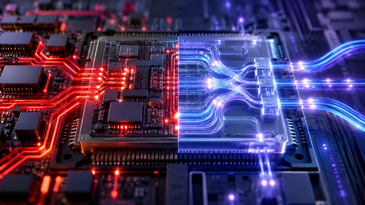
Photonic computing is an emerging approach that uses light, rather than relying entirely on electrical signals, to transmit information or perform selected calculations. By using photons and optical components, researchers aim to improve bandwidth, reduce certain data-transfer bottlenecks, and potentially increase energy efficiency in future computing systems. However, optical communication and optical computation are different technologies, and light-based systems do not automatically outperform conventional electronic chips. This guide explains how photonic chips work, where silicon photonics is already useful, the challenges of optical processing, and whether future processors could combine light with traditional electronics.
What Photonic Computing Means?
Photonic computing refers to architectures that use photons, or particles of light, to represent information and perform selected processing operations. In optical computing, components such as waveguides, interferometers, modulators, and photodetectors help manipulate light-based signals. Many practical designs combine optical components with electronic circuits rather than replacing conventional processors completely. These hybrid systems can use electronics for control, memory, and complex logic while using photonics for high-bandwidth communication or specialized mathematical operations.
At the chip level, photonics can involve optical links, modulators, waveguides, photodetectors, and supporting electronic circuitry integrated within or near processor packages. Intel’s silicon photonics technology provides a practical example of optical components designed for high-bandwidth communication in computing infrastructure. While optical interconnects are already used commercially, fully optical general-purpose logic remains substantially less mature. Current developments increasingly focus on advanced optical connectivity and specialized photonic processing rather than replacing every transistor in a conventional CPU.
Why Light is Attractive for Chips?

Electrical interconnects can experience resistive losses, signal attenuation, and interference, especially as data rates increase and connections become longer or more densely packed. Optical waveguides transmit information using light, which is not affected by electrical resistance in the same way as current flowing through metal wires. This can provide advantages in bandwidth density, signal integrity, and energy efficiency for suitable communication distances. However, optical links also require lasers, modulators, photodetectors, and supporting electronic circuits. Their total power consumption must therefore be evaluated against electrical alternatives for the same workload and connection distance.
Light also enables wavelength-division multiplexing (WDM), a technique that transmits multiple independent data channels through one optical fiber or waveguide using different wavelengths of light. These wavelengths are often in the infrared spectrum rather than the visible colors people normally see. WDM can increase the amount of information carried by a single optical connection without requiring a separate physical path for every channel. The research organization imec explains how silicon photonics can address data-center bandwidth demands, including the use of optical multiplexing and advanced packaging for future computing infrastructure.
- Higher Bandwidth Density: Multiple wavelengths can share one path, helping avoid pin and routing limits.
- Lower Interconnect Energy: Optical links can reduce the power spent moving bits between chiplets and racks.
- Less Heat From Data Movement: Efficient optical interconnects may reduce energy losses associated with high-bandwidth data transmission, potentially lowering some heat-generation and cooling requirements. However, lasers, optical tuning circuits, and electronic interfaces still consume power and generate heat, so the overall thermal benefit depends on the system design.
- Better Signal Integrity: Optical channels are less affected by electromagnetic interference and resistive noise.
These strengths matter most when data movement, not arithmetic, dominates the power and latency budget.
How Photonic Chips Work at A High Level?
A typical silicon photonics stack combines optical and electronic components on the same package. Lasers generate light, modulators encode data onto that light, waveguides route it, and photodetectors convert it back into electrical signals where needed.
Photonic systems can use external lasers or integrate light sources more closely with optical circuits, depending on their architecture. External laser configurations can provide design and thermal-management flexibility, while integrated laser solutions may reduce optical coupling complexity. Although generating light efficiently in conventional silicon presents material challenges, commercial and experimental photonic platforms have demonstrated integrated laser technologies. For example, Intel has demonstrated optical input/output chiplets that integrate laser sources with photonic and electronic components. The choice between integrated and external lasers depends on manufacturing methods, reliability, temperature control, cost, and power efficiency.
Key Building Blocks
Each block has its own efficiency, footprint, and manufacturability constraints. Progress comes from improving each part without breaking compatibility with mainstream fabrication.
- Laser Sources: Provide stable light but can add cost and require careful temperature control.
- Optical Modulators: Convert electrical bits into changes in amplitude or phase on a light wave.
- Waveguides and Couplers: Route photons on chip and connect to fibers or neighboring chiplets.
- Photodetectors: Turn light back into electrical signals for logic and memory interfaces.
- Optical Switches: Steer traffic across a photonic network on chip or between chiplets.
Together these parts form an optical data plane that can sit beside conventional electronic compute.
Photonic Interconnects Versus Photonic Computing
It helps to separate two ideas that often get blended together. Photonic interconnects focus on moving data using light, while photonic computing aims to perform operations in the optical domain.
Optical communication links are already established in data-center networking, and researchers are developing designs that move optical connections closer to processors and memory systems. Performing calculations with light introduces additional challenges because a practical computing architecture must support reliable nonlinear operations, information storage, signal control, and scalable integration. A peer-reviewed study on optical neural networks and their challenges discusses the progress of optical computing architectures and the difficulties associated with nonlinearity, computational density, and large-scale implementation. These limitations help explain why optical connectivity has progressed further commercially than fully optical general-purpose computing.
| Technology | Main Function | Potential Advantage | Key Limitation | Development Status |
|---|---|---|---|---|
| Optical Interconnects | Transmit data using light between computing components | High bandwidth and potentially lower energy per bit over suitable distances | Laser power, optical conversion, coupling losses, and packaging | Commercially used in data-center networking; closer chip integration is advancing |
| Optical Switching | Direct optical signals between communication paths | High-capacity traffic routing with reduced electrical signal conversion in suitable designs | Switching control, insertion loss, integration, and scalability | Established in optical networking, with newer chip-scale designs under development |
| Analog Photonic Accelerators | Perform selected mathematical operations using optical signals | Parallel processing of operations such as matrix multiplication | Numerical precision, noise, calibration, and electronic conversion overhead | Demonstrated in research prototypes |
| Optical Logic | Perform logical operations using optical components | Potential high-speed operations in specialized architectures | Optical nonlinearity, memory, fanout, and system integration | Primarily experimental for general-purpose computing |
This comparison shows why most practical deployments start with communication first, then expand into compute where it fits.
Where Photonics Can Help Most?
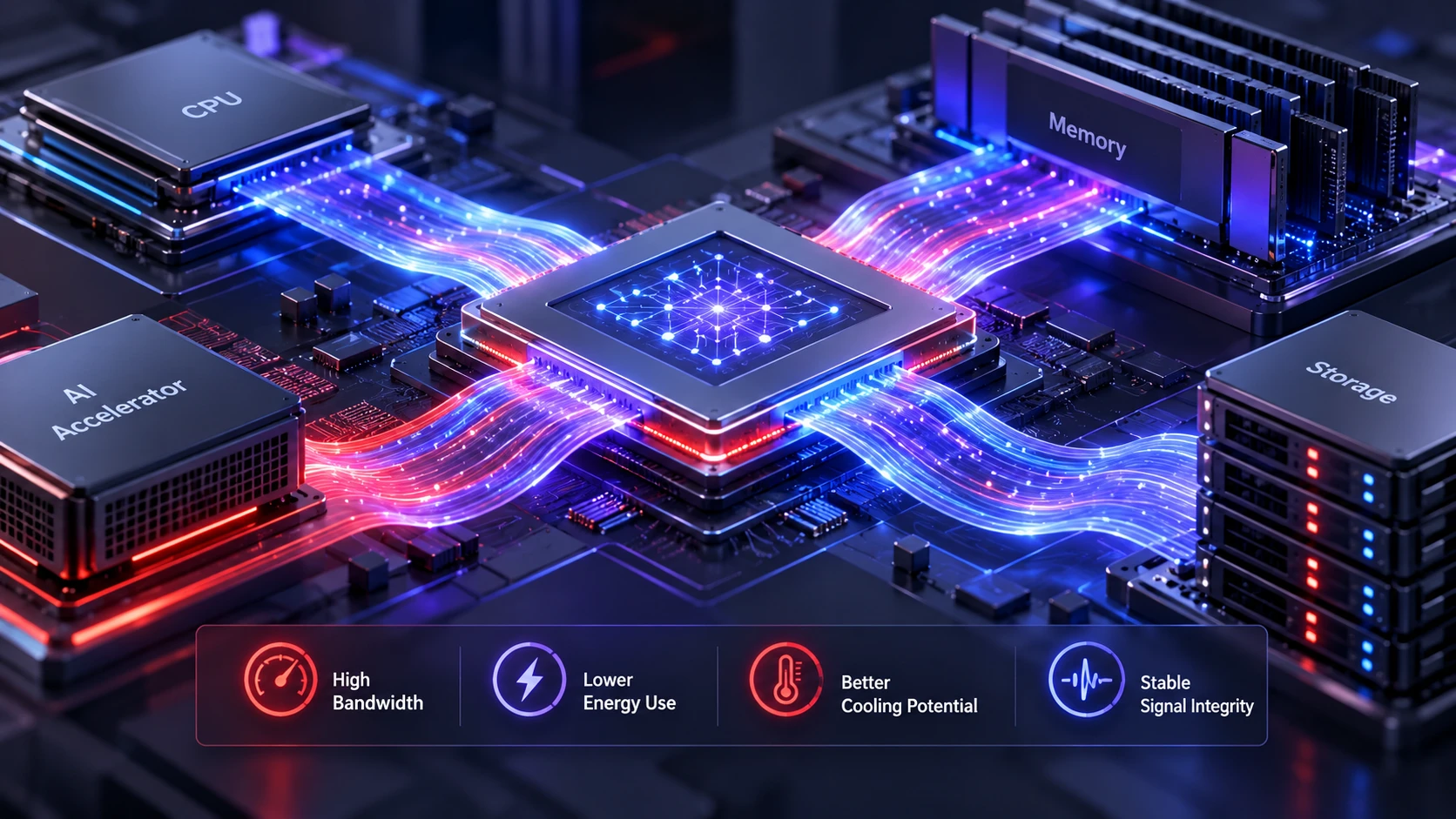
Modern computing systems can experience performance and energy bottlenecks when large amounts of information must move between processors, memory, accelerators, and other hardware components. Photonic interconnects may help address some of these limitations by supporting dense, high-bandwidth data transmission over suitable connection distances. A 2025 study published in Nature Photonics on three-dimensional photonic integration for interchip data links demonstrated an integrated optical communication platform designed for high-bandwidth, energy-efficient interchip connectivity. Such research illustrates the potential benefits of combining optical and electronic components in future AI and high-performance computing systems.
Photonic computing may also be useful for specialized workloads involving highly parallel mathematical operations, particularly when optical interference can perform selected calculations efficiently. Research into integrated photonic accelerators has demonstrated optical hardware for targeted computational tasks, providing evidence that photonic processing can extend beyond communication. However, these systems often depend on analog signal behavior and must address numerical precision, noise, calibration, and electronic interface overhead. Their potential advantages should be evaluated against conventional accelerators using complete workload-level measurements.
Best Fit Workload Traits
- Bandwidth Bound Pipelines: Systems where moving tensors and activations dominates energy use.
- Highly Parallel Linear Operations: Matrix multiplications that map well to optical interference patterns.
- Long Reach Links: Chip to chip and chip to rack paths where copper becomes inefficient.
- Thermally Constrained Designs: Platforms where cooling headroom is limited and interconnect heat is costly.
These conditions can arise in AI infrastructure, high-performance computing, and distributed data-center architectures, especially when large volumes of information move between processors and accelerators. Different AI workloads also place different demands on network bandwidth, memory, latency, and power consumption. Our comparison of training vs inference AI data centers explains how hardware and infrastructure requirements change between these workloads. Understanding those differences can help identify where future photonic interconnects may offer meaningful advantages.
Core Limits That Still Hold Photonics Back
One of the main challenges of photonic computing is implementing reliable logic and nonlinear processing. Conventional electronic transistors provide compact switching, signal amplification, and digital control, while many optical components are naturally suited to linear operations. Researchers are developing optical nonlinear devices and hybrid electronic-photonic architectures, but achieving scalable, low-power, general-purpose optical logic remains difficult. Device size, signal loss, noise, and control requirements further complicate the design of complete photonic processors.
Memory is another major limitation. Conventional computing systems rely on electronic memory technologies that can store and retrieve information efficiently, while practical optical alternatives remain more specialized. Hybrid photonic systems often convert signals between electrical and optical forms to interact with processors and memory. These conversions introduce additional power consumption, latency, and hardware complexity. As a result, photonic computing must deliver sufficient processing or communication benefits to justify the overhead of integrating optical components into an electronic system.
- Device Footprint: Some photonic components are larger than transistor scale features.
- Conversion Overhead: Electrical to optical and optical to electrical conversions can add latency and power draw.
- Thermal Sensitivity: Resonant devices can drift with temperature, requiring tuning and control loops.
- Manufacturing Complexity: Co integrating photonics with advanced CMOS nodes raises yield and test challenges.
Solving these constraints is less about one breakthrough and more about maturing an entire ecosystem of processes, packaging, and design tools.
What A Realistic Path to Light Based Chips Looks Like?
One plausible path toward wider photonic computing adoption is through hybrid architectures that combine electronic processing with optical communication and specialized acceleration. Conventional processors can continue handling flexible logic, control, and memory operations, while photonic components support high-bandwidth connections or carefully selected computational workloads. Different processors are already optimized for different functions, as explained in our guide to CPU vs GPU vs NPU. Photonic technologies could become another specialized part of this broader computing ecosystem rather than replacing all existing processor types.
Chiplet based architectures make this transition easier. A system can add a photonic I O chiplet, then expand to optical switching fabrics, and only later consider deeper optical compute elements if they prove reliable and cost effective.
- Adopt Optical I/O Near the Package: Evaluate optical input/output connections for communication paths where electrical interconnects face significant bandwidth, signal-integrity, or power-efficiency limitations. Optical solutions may be especially useful for longer-reach, high-bandwidth connections between processors, chiplets, boards, or racks. The decision should account for laser power, electrical-to-optical conversion, packaging, latency, and total system energy rather than assuming that every electrical connection should be replaced.
- Scale to Chiplet and Rack Fabrics: Use photonic switching and wavelength multiplexing to reduce network congestion and cabling limits.
- Add Optical Assist for Targeted Kernels: Introduce photonic accelerators for narrow, high impact operations after calibration and monitoring are robust.
This staged approach reduces risk and aligns with how data center hardware evolves.
Real-World Progress in Photonic Chips
Research and industry demonstrations show that some elements of photonic computing are already functioning in practical hardware. In 2024, Intel demonstrated an optical compute interconnect chiplet integrated with a conventional CPU, showing how optical data transmission could support high-bandwidth communication in future computing systems. This demonstration focused on optical connectivity rather than replacing the CPU’s electronic logic.
Academic research has also demonstrated specialized optical processing hardware. A 2025 study published in Nature described an integrated photonic accelerator designed to perform particular computational operations with very low latency. Such systems illustrate the potential of light-based processing, but they should not be confused with commercially available, fully optical general-purpose CPUs.
These developments suggest that optical interconnects and specialized photonic accelerators may advance alongside conventional electronics. Their broader adoption will depend on measured performance, reliability, manufacturing cost, and the ability to integrate with existing computing infrastructure.
Design and Deployment Considerations
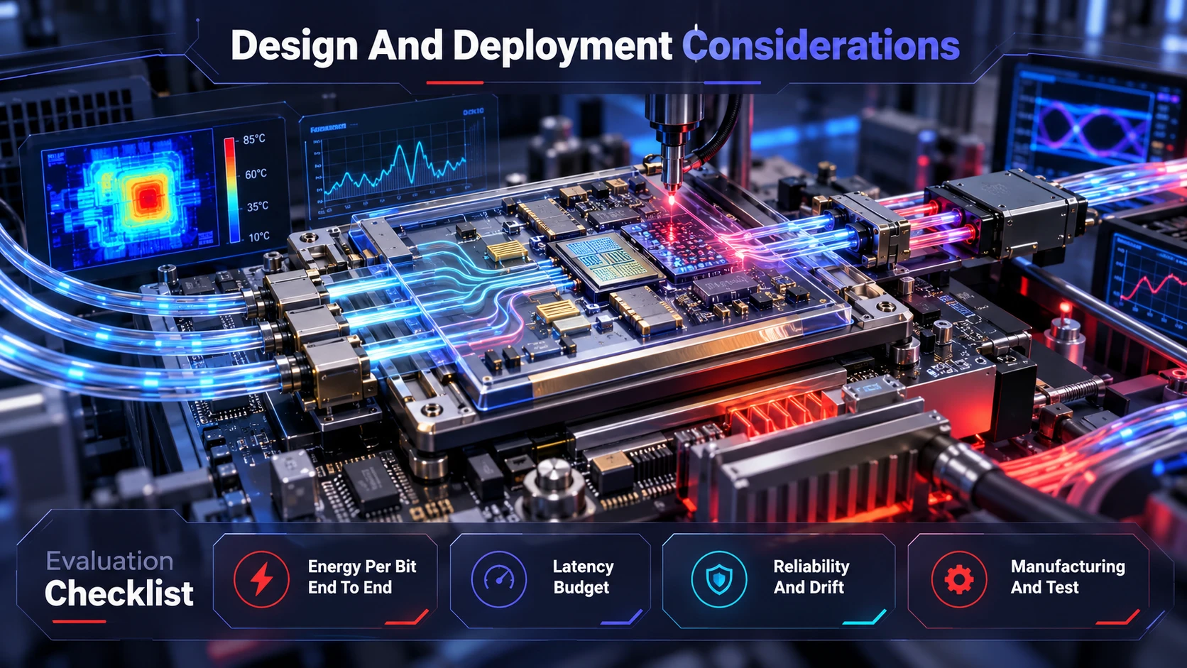
The success of photonic computing depends on more than the performance of individual optical devices. System designers must consider optical coupling losses, package integration, thermal stability, control electronics, and reliable manufacturing methods. Research from imec on high-density co-packaged optics explains the engineering challenges of connecting optical circuits to fibers and integrating photonic components into advanced semiconductor packages. These considerations influence whether laboratory demonstrations can be developed into reliable, scalable hardware.
System architects must evaluate end-to-end energy consumption rather than relying only on optical component specifications. A photonic link that performs efficiently in isolation may offer a smaller system-level advantage once laser power, thermal tuning, electronic conversion, and packaging requirements are included. Advanced semiconductor packaging and testing also influence integration reliability, manufacturing yields, and long-term performance. Our overview of semiconductor packaging and testing explains why these manufacturing processes are important when integrating advanced chip technologies.
Evaluation Checklist
- Energy Per Bit End to End: Include laser efficiency, tuning power, and receiver amplification.
- Latency Budget: Account for serialization, conversion stages, and routing control loops.
- Reliability and Drift: Plan for monitoring, calibration, and redundancy where resonances shift.
- Manufacturing and Test: Ensure wafer level testing, optical probing, and yield learning are feasible.
These practical factors often determine whether photonics delivers real system level gains.
Conclusion
Photonic computing is not a simple swap of electrons for photons across an entire processor. Light is strongest where bandwidth, distance, and heat from data movement are the limiting factors, which is why optical interconnects are leading the way.
Future chips can use light more deeply, but the likely outcome is hybrid computing where photonics complements electronics. As packaging, control, and manufacturing mature, photonic links and optical switching can become common building blocks in high performance and AI focused systems.
Frequently Asked Questions
Is Photonic Computing Faster Than Electronic Computing?
Photonic signals can move data quickly and with low loss, which helps when communication is the bottleneck. Raw compute speed depends on the full design, including conversions and control circuitry. Many gains come from higher bandwidth and lower energy per bit rather than clock speed alone.
Will CPUs Be Fully Optical in the Near Future?
Fully optical general purpose CPUs are unlikely in the near term because photonics struggles with compact logic, memory, and strong switching behavior. Hybrid designs are more practical, using optical links and switching while keeping transistor logic for control and branching. That approach can still deliver meaningful efficiency improvements.
What is the Biggest Challenge for Photonic Chips?
The hardest issues are system level, not just device level. Packaging, thermal stability, and conversion overhead can erase theoretical advantages if not engineered carefully. Cost, yield, and testing also matter because photonics must scale like mainstream semiconductor manufacturing to become widespread.
Is Photonic Computing the Same As Quantum Computing?
No. Photonic computing and quantum computing are different approaches, although both can use light. Conventional photonic computing generally uses optical signals to transmit information or perform selected classical computations, such as matrix operations. Photonic quantum computing uses quantum states of light to encode and manipulate quantum information. The two technologies have different operating principles, hardware requirements, and applications. A chip that uses optical interconnects or photonic accelerators is not automatically a quantum computer.